Modern devices are becoming smaller, more sensor-intensive and more connected. At the same time, conventional assembly technology is reaching its limits. Every sensor, every circuit board and every contact element is a separate component that takes up space, has to be mounted and represents a potential point of failure. On curved or irregularly shaped surfaces, conventional electronics can in any case only be accommodated with considerable effort.
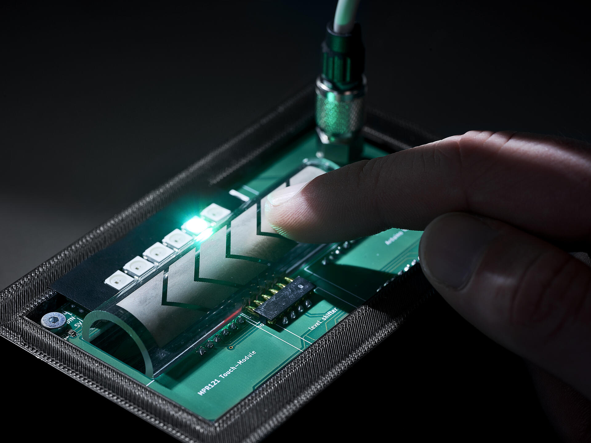
This is where printed electronics comes in. Using the process developed at the ITZ, binder applies functional layers directly onto the component – for example onto substrates made of plastic, metal, glass or ceramic. The company employs high-precision screen and pad printing with conductive pastes based on silver, copper, carbon or PEDOT:PSS, as well as dielectric pastes. Multilayer printing produces conductor tracks, heating elements or sensors, including on three-dimensionally shaped and curved surfaces where conventional circuit boards reach their limits.
The applications are wide-ranging. In mechanical engineering, printed sensors supply data for condition monitoring and predictive maintenance; in operating interfaces, printed touch and force sensors replace mechanical buttons; and printed heating elements keep components reliably at temperature. The benefit is similar in every case: fewer individual parts, lower weight, more compact installation spaces and greater design freedom. Function and housing become one and the same part.
“Printed electronics shifts the limit of what a single component can achieve. We apply conductor tracks, heating functions or sensor technology directly onto the surface, saving a whole range of individual parts and creating intelligent components. At the ITZ, we develop these processes through to application maturity. The binder group then turns the functional prototype into a production-ready solution. This path from idea to series production is something pure printing specialists cannot offer in this form,” says Dr.-Ing. Martin Ungerer, Team Leader Printed Electronics at binder ITZ.
This is precisely where the strength of the binder group network comes into play. While the printing processes are researched and brought to series maturity at the ITZ, binder solutions handles the customer-specific implementation. Thanks to the vertically integrated structure – from cable assembly through precision-turned parts and zinc die-casting to the complete assembly – the printed functional layer can be combined with connectors and connection technology to form a coordinated overall system. Customers therefore do not receive an isolated printed component, but a seamless solution from a single source, from the prototype to the series-ready part.
With the ITZ in research and development and binder solutions in implementation, the binder group covers the entire path, from process development to the functionalised series component. For customers who need to accommodate function in the smallest of spaces and on demanding geometries, the connector specialist thus becomes a development partner for the next generation of devices.